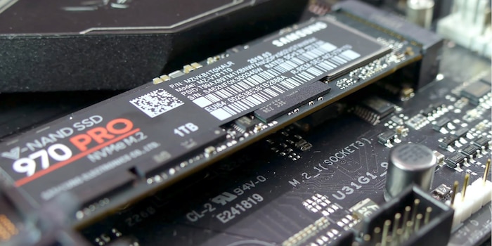
SSD operation is a complex business
SSDs are increasingly replacing hard disks as the main form of mass storage. Their speed and mobility offer undeniable advantages. Data is read and written electrically, not mechanically. How do they work?
Every year sees the emergence of a new generation of processors that are more than promising. The average user doesn't really notice, but the same can't be said for SSDs. The switch from HDD to SSD is noticeable, regardless of how it's used.
I used to turn on my computer and go and get a coffee while it booted up.... I fell head over heels in front of a notebook with an SSD drive. It was like going from a regional train to a TGV. Or from walking to running. Anyway, you get the idea.
But what makes SSD drives so fast? Unlike hard drives, they don't have read heads, write heads or rotating platters. Each block can be accessed at the same speed. It doesn't matter whether they're next to each other or on another module. So there's no point in defragmenting them. Access times are shorter, and read and write speeds are higher.
I got the idea of looking into how SSDs work when writing my article devoted to the history of the hard disk. I first wanted to write about their lifespan. As I did my research, I started to get annoyed. You read everywhere that NAND flash memory (the storage technology used in SSDs) wears out over time, but nobody explains exactly how. What on earth are the physical processes that take place?
So I've decided to dedicate an article to it. Once you understand how these discs work, their wear and tear will make sense. And you'll also be able to clear up some previously unanswered frequently asked questions. Why SSDs slow down when they run out of storage space, for example.
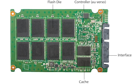
A word of warning before we dive into the heart of the matter: some passages are highly technical. A solid state drive consists of a board with an interface (SATA, PCIe, SATA-Express or other), NAND flash memory, cache memory depending on the drive, and a controller on which the firmware is located. It is controlled via a protocol (AHCI or NVMe). Let's start with NAND flash memory.
What is NAND flash memory
In contrast to hard disks, data is electronically read from and written to NAND flash memory. This is distinguished by its high storage capacity and good data protection. It does what platters do on a hard disk: it backs up data permanently by creating a voltage.
Bit lines and word lines

A NAND block consists of bit lines and word lines. The bit lines are parallel. They are made of silicon and are separated by a technique called "shallow trench isolation" (STI). The word lines, made of polysilicon, are perpendicular to the bit lines. The control gate is placed on these lines. The memory cell is located where the bit line and word line intersect.
The individual memory cells are so-called Floating Gate Metal Oxide Semiconductor Field Effect Transistors (FGMOS). The floating gate is located between the control gate and the bit line. It is an electrically insulated semiconductor layer that stores charge and floats in the insulation layer. The electrons in the floating gate do not discharge for two to ten years, even when not energised.
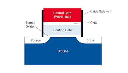
Let's take a closer look at the interface between the bit line and the word line, along the word line to be precise. The control grid surrounds the floating grid. The two grids are separated by an oxide-nitride-oxide (ONO) layer. Below the floating gate is the tunnel oxide (non-conductive), then the bit line with the source and drain.
Pages, blocks, planes and "dies"
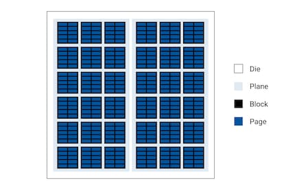
The memory cells in a word line are grouped together in a page. Pages are the smallest units that can be read from or written to an SSD. Depending on the manufacturing process or the type of flash memory, pages can be 2KB, 4KB, 8KB or 16KB.
Several pages are grouped together in blocks. Each block comprises between 128 and 256 pages. A block is the smallest unit that can be erased. Technically, erasure could also take place at page level, but the voltage required would be so intense for the memory cells that the lifespan would be further shortened. I provide more information on the use of memory cells below.
The blocks, meanwhile, are generally spread over two planes per flash module (also known as "dies"). The modules come to rest on the board. There they are connected to the controller via four to ten channels.
Small aside: the slowdown of SSDs
As I just mentioned, data erasure is only possible at the block level. In order to refresh a page, the contents of the block, on which the page is located, must be copied. The block must then be deleted, and the contents of the old block saved on a new block with the updated page. SSD data can be read and written very quickly, but erasing and rewriting it is much slower (much faster than hard disks, though). When the SSD is almost full and there are no free pages, it first has to look for blocks that can be erased. SSDs can therefore slow down as they fill up. Today's controllers are equipped with several mechanisms to counter this phenomenon. We'll look at how the controller works a little later.
How data is read and stored
To simplify, data in a flash memory is recorded when electrons are placed on or removed from the floating gate. The bits are read using the voltage. When electrons are present on the floating gate, the bit has a value of 0. When none are present, the bit has a value of 1. Memory cells are considered empty or erased when they have a value of 1 and written when they have a value of 0.
.
Let's take a closer look at this and start with reading.
Reading
When reading, the key element is the negative charge of the floating gate (when electrons are present in the floating gate), which opposes the positive voltage propagating through the control gate. This means that at a value of bit 0, more voltage is needed to exceed the limit value and allow the current to flow through the control grid. This voltage is called VT0. The voltage required at a value of bit 1, when the current passes through the control gate, is called VT1. In order to read the value, the voltage must lie between VT0 and VT1 (it is called VR), it must be sent through the control gate, and the current must be measured. If the current passes through the control gate, you get a bit value of 1. If it doesn't, you get a bit value of 0. This is how SLC NANDs work. In MLC or TLC NANDs, various VRs have to be measured. I provide more information on SLC, MLC and TLC in the relevant paragraphs.
Erasing
When erasing, the electrons are removed from the floating gate, and the bit value returns to a normal value of 1. There is no electrical contact between the electrons and the floating gate. So how can they be removed? They have to pass through the oxide layer, which separates the floating gate from the bit line. This is where the tunnel effect comes into play. A high negative voltage is applied to the source and control grid. Electrons are attracted to the floating grid and transferred to the source by the tunnel effect.
Writing and programming
When writing, electrons are transferred to the floating gate, and a bit value of 0 is obtained. When a high positive voltage is applied to the control gate and another is simultaneously applied to the drain, electrons can pass through the oxide layer and reach the floating gate. This process is called hot electron injection.
SLC, MLC and TLC memories
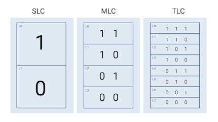
A memory cell generally has only two states: charged or uncharged, i.e. written (programmed) or deleted. This information measures one bit. Storing multiple states can increase memory density. This can be done at various voltage levels. For the single-level cell (SLC), a single bit is stored per cell. Multi-level cells (MLC) store two bits per memory cell and triple-level cells store three bits per cell. The choice of cell affects read and write speed, as well as the durability of the drive.
The SLC memory
Since only one bit is stored per memory cell, the failure rate is very low. Only two voltage levels are required for reading and writing, which increases speed and reduces power consumption. SLC flash memories are considered to have a lifetime of 100,000 write cycles per block.
MLC memory
High memory density means fewer memory cells and more capacity. MLC flash memory is cheaper to manufacture, but takes longer to read and write, and has a shorter lifespan. The memory cells must be able to withstand four voltage levels, and the controller must be able to read them. As a result, the memory cells wear out more quickly and the read and write processes take longer because they are more complex. On the other hand, this complexity reduces the number of errors. Controllers need to perform better. MLC flash memories are considered to have a lifetime of 3000 write cycles per block.
TLC memory
TLC flash memory differs more clearly from SLC and MLC memory. It costs even less to manufacture than MLC. Memory cells have to withstand eight voltage levels. Reading takes around four times as long, and writing six times as long as with SLC memory. We're talking about a lifetime of 1,000 write cycles per block.
Another little aside: the lifespan of an SSD drive
As I've already mentioned, writing data is only possible to an empty or erased memory cell. Overwriting data itself is impossible. Data must first be erased and then rewritten to be modified. The lifetime of an SSD drive is therefore measured in write cycles.
During writing, the floating gate is subjected to a high voltage. This is a necessary step in order to ensure current flow through the oxide layer. The insulation layer is damaged with each write access; eventually it no longer functions properly. The data can no longer be stored reliably, and the memory cell becomes unusable. This is also the reason why MLC and TLC flash memories do not last as long as SLC memories. Writing requires a higher voltage, which causes more damage to the oxide layer. In addition, there are fewer differences in voltage levels when reading. When the oxide layer no longer insulates properly, reading is no longer guaranteed.
Many tests and articles have been devoted to the lifespan of SDD drives and their write and erase cycles. I won't go into detail, but most tests show that SSD drives often last much longer than the manufacturer states. For example, a 250GB Samsung 850 Pro achieved astonishing results in c't magazine's durability test (in German). In all, 9.1 petabytes were written to the SSDs, equivalent to more than 620 years' worth of daily office tasks.
The controllers and the processor
As we've seen, the flash memory in SSDs has a few advantages over hard drives. As I've described below, however, SSD drives require some very complex control mechanisms in order to function. This is where controllers and firmware come in. Controllers often have built-in RAM to help them process data. Many drives also have a cache that acts as a buffer. The controller governs processes such as rubbish collection or wear management, the main ones of which are listed below. Unfortunately, I can't go into more detail about the controller's functions. As SSD drives are mainly distinguished by the functions of their controller and firmware, manufacturers are fairly stingy with information.
Write amplification
SSDs write data to pages but erase blocks. As a result, there are always more writes than an update requires. For example, when I edit a 16k file, the block where those 16k are has to be completely erased and rewritten. Depending on the number of pages per block and the size of the pages, a lot more data needs to be written than the 16 kB in question. Write amplification describes the proportion of data to be written in relation to the actual data. Rubbish collection and TRIM aim to counter this effect.
Garbage collection
Garbage collection is a background process used to counter SSD slowdowns as memory capacity decreases. Partial blocks are copied and assembled into new, complete blocks. The old blocks are then erased, freeing them up for rewriting. This does not limit accesses to the SSD.
The TRIM
In order for you to better understand the function of TRIM, let me first explain how data is erased from a hard drive. In fact, they are not immediately deleted. The operating system informs the hard disk that the physical location may be overwritten during the next backup. This is why data that has already been deleted can be recovered. However, the operating system does not need to tell the SSD where the data is being written and in what state the pages or blocks are. The TRIM command allows the operating system to communicate to the SSD controller that it no longer needs to write certain data when a block is deleted or rewritten. The amount of data written is therefore reduced, and the lifespan increased.
Wear management (wear leveling)
The wear leveling function prevents specific blocks from being written and erased more frequently than others. It increases the lifespan, because these blocks are not worn out prematurely. On the other hand, it can lead to write amplification. In order for write cycles to be distributed evenly, a block must sometimes be deleted, even if its contents have not been updated. Wear management must be balanced. SSDs have what is known as a dedicated reserve area. This is an area of data that the operating system does not see. It also makes it easier to replace damaged blocks.
The future
Despite some problems, NAND flash memories have huge advantages over hard disks. I've touched on two of these challenges: lifespan and slowdowns. NAND flash drives also take up a lot of space. The capacity of current NAND flash memories could be increased by reducing the size of the structures. Unfortunately, the smaller they are, the more sensitive the floating gate is, and the more electricity the drive consumes. Smaller structures limit the number of electrons in the memory cells and require a thinner oxide layer, which wears out more quickly. This increases the likelihood of errors and reduces the number of write cycles.
The other methods of increasing memory in a limited space have been mentioned in the paragraphs devoted to MLC and TLC memories. But there is a physical limitation here too. To finish my article, I'd like to look again at two approaches that have increased the memory capacity and speed of SSDs and will continue to do so in the future.
3D NAND or V-NAND memory
While in NAND memories the memory cells are placed next to each other, in a 3D NAND memory they are superimposed and connected on a vertical plane, which increases memory capacity. Vertical positioning increases space across the width. The electrons also have more space in the floating grid. As a result, less voltage is required for erasing, writing and reading. Errors are also less likely to occur, as the floating grid accommodates more electrons and reaches more voltage levels, making it easier to read. This 3D structure is already standard in many SDD drives.
The NVMe protocol
SSD drives can be linked to a variety of interfaces. In addition to the old SATA and SAS standards, PCIe is gaining in popularity, as the SATA connection and AHCI protocol limit the speed of SSD drives (transfer rates do not go beyond 600 MB/s). The PCIe ("Peripheral Component Interconnect Express") interface and the NVMe protocol offer better transfer rates than SATA or SAS, because a greater number of channels promote data flow. Unlike SATA, a PCIe-3.0 connection, for example, offers a transfer rate of 1,000 MB/s on one transmission channel.
The AHCI protocol is no longer suited to these high transfer rates, which is why the NVMe protocol was created. It is claimed to reduce delays by 50%, as the design of an NVMe stack driver is simpler and more efficient. The protocol also offers 65536 I/O queues with 65536 commands, whereas AHCI only has a queue of 32 commands. This means that several commands can be processed in parallel. The NVMe protocol makes it possible to transfer large volumes of data quickly, boot operating systems promptly, shorten program loading times and improve system response times.
The theoretical transfer rate of 4 GB/s with PCIe 3.0 over four transmission channels is already almost exceeded. The new Samsung 970 Pro, for example, achieves maximum values of 3.5 GB/s. The PCIe-4.0 standard was launched in 2017. It provides up to 2,000 MB/s per transmission channel. The PCIe 5.0 standard is already under development. Data rates are set to double again. Not only will mass storage devices have more storage space in the future, they will also be much faster.
From big data to big brother, Cyborgs to Sci-Fi. All aspects of technology and society fascinate me.
Interesting facts about products, behind-the-scenes looks at manufacturers and deep-dives on interesting people.
Show all